- 您现在的位置:买卖IC网 > Sheet目录328 > IDT70125L25JG (IDT, Integrated Device Technology Inc)IC SRAM 18KBIT 25NS 52PLCC
�� �
�
�IDT70121/IDT70125�
�High-Speed� 2K� x� 9� Dual-Port� Static� RAM� with� Busy� &� Interrupt�
�Industrial� and� Commercial� Temperature� Ranges�
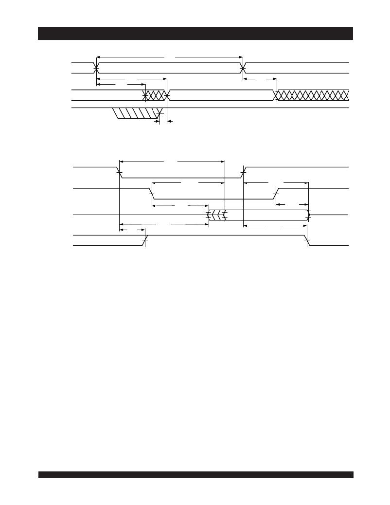
�Timing� Waveform� of� Read� Cycle� No.� 1,� Either� Side� (1,2,4)�
�t� RC�
�ADDRESS�
�t� OH�
�t� AA�
�t� OH�
�DATA� OUT�
�PREVIOUS� DATA� VALID�
�DATA� VALID�
�BUSY� OUT�
�2654� drw� 05�
�t� BDD�
�(3,4)�
�Timing� Waveform� of� Read� Cycle� No.� 2,� Either� Side� (5)�
�t� ACE�
�CE�
�OE�
�DATA� OUT�
�t� AOE�
�t� LZ� (1)�
�(4)�
�t� HZ� (2)�
�VALID� DATA�
�t� HZ� (2)�
�I� CC�
�CURRENT�
�t� PU�
�t� LZ� (1)�
�50%�
�t� PD�
�(4)�
�50%�
�I� SS�
�2654� drw� 06�
�NOTES:�
�1.� Timing� depends� on� which� signal� is� aserted� last,� OE� or� CE� .�
�2.� Timing� depends� on� which� signal� is� deaserted� first,� OE� or� CE� .�
�3.� t� BDD� delay� is� required� only� in� a� case� where� the� opposite� port� is� completing� a� write� operation� to� the� same� address� location.� For� simultaneous� read� operations�
�BUSY� has� no� relationship� to� valid� output� data.�
�4.� Start� of� valid� data� depends� on� which� timing� becomes� effective� last,� t� AOE,� t� ACE,� t� AA,� or� t� BDD.�
�5.� R/� W� =� V� IH� ,� CE� =� V� IL� ,� and� OE� =� V� IL� ,� and� the� address� is� valid� prior� to� other� coincidental� with� CE� transition� LOW.�
�7�
�发布紧急采购,3分钟左右您将得到回复。
相关PDF资料
IDT7014S12JG
IC SRAM 36KBIT 12NS 52PLCC
IDT7015L35G
IC SRAM 72KBIT 35NS 68PGA
IDT7016L35G
IC SRAM 144KBIT 35NS 68PGA
IDT7019L20PFI
IC SRAM 1.125MBIT 20NS 100TQFP
IDT7024L55G
IC SRAM 64KBIT 55NS 84PGA
IDT7025L55G
IC SRAM 128KBIT 55NS 84PGA
IDT70261L20PFI
IC SRAM 256KBIT 20NS 100TQFP
IDT7026L20G
IC SRAM 256KBIT 20NS 84PGA
相关代理商/技术参数
IDT70125L25JG8
制造商:Integrated Device Technology Inc 功能描述:IC SRAM 18KBIT 25NS 52PLCC
IDT70125L25JGI
制造商:IDT 制造商全称:Integrated Device Technology 功能描述:HIGH-SPEED 2K x 9 DUAL-PORT STATIC RAM WITH BUSY & INTERRUPT
IDT70125L25L52
制造商:未知厂家 制造商全称:未知厂家 功能描述:x9 Dual-Port SRAM
IDT70125L35J
功能描述:IC SRAM 18KBIT 35NS 52PLCC RoHS:否 类别:集成电路 (IC) >> 存储器 系列:- 标准包装:72 系列:- 格式 - 存储器:RAM 存储器类型:SRAM - 同步 存储容量:9M(256K x 36) 速度:75ns 接口:并联 电源电压:3.135 V ~ 3.465 V 工作温度:-40°C ~ 85°C 封装/外壳:100-LQFP 供应商设备封装:100-TQFP(14x14) 包装:托盘 其它名称:71V67703S75PFGI
IDT70125L35J8
功能描述:IC SRAM 18KBIT 35NS 52PLCC RoHS:否 类别:集成电路 (IC) >> 存储器 系列:- 标准包装:72 系列:- 格式 - 存储器:RAM 存储器类型:SRAM - 同步 存储容量:9M(256K x 36) 速度:75ns 接口:并联 电源电压:3.135 V ~ 3.465 V 工作温度:-40°C ~ 85°C 封装/外壳:100-LQFP 供应商设备封装:100-TQFP(14x14) 包装:托盘 其它名称:71V67703S75PFGI
IDT70125L35JG
制造商:IDT 制造商全称:Integrated Device Technology 功能描述:HIGH-SPEED 2K x 9 DUAL-PORT STATIC RAM WITH BUSY & INTERRUPT
IDT70125L35JGI
制造商:IDT 制造商全称:Integrated Device Technology 功能描述:HIGH-SPEED 2K x 9 DUAL-PORT STATIC RAM WITH BUSY & INTERRUPT
IDT70125L35JI
功能描述:IC SRAM 18KBIT 35NS 52PLCC RoHS:否 类别:集成电路 (IC) >> 存储器 系列:- 标准包装:72 系列:- 格式 - 存储器:RAM 存储器类型:SRAM - 同步 存储容量:9M(256K x 36) 速度:75ns 接口:并联 电源电压:3.135 V ~ 3.465 V 工作温度:-40°C ~ 85°C 封装/外壳:100-LQFP 供应商设备封装:100-TQFP(14x14) 包装:托盘 其它名称:71V67703S75PFGI